


News


Control of Wafer Scanners: Methods and Developments
Today's information economy, including paradigms such as the Internet of Things and the era of big Data, is built on half a century of technological developments in the semiconductor industry based on Moore's Law. The main technological enabler behind these developments is widely believed to be the lithography process, as it provides the current standard for producing microchips in a cost-effective manner. Photolithography is a key process in wafer scanners, the machines used to make microchips.
With a list price of $10,000,000- $150,000,000, lithography machines consist of a number of highly complex mechatronics systems that combine high throughput with high precision. In terms of throughput, modern lithography machines can process about 280 wafers per hour, where it takes less than 10 seconds to expose a 300 mm wafer containing about 100 exposure fields. Each field allows complex processor chips to be built through a scanning process. Scanning is done by commanding a series of connected point-to-point motions, during which the tracking specifications of the scanner motion system are mostly in the (sub-) nanometer range.
The lithography machine consists of several main subsystems. For example, light sources, lighting optics, mask and wafer systems, and material handling robots, these subsystems are high-precision mechatronics systems that make extensive use of advanced controls to meet specifications.
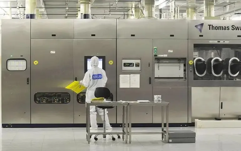
Wafer Scanner Scanner
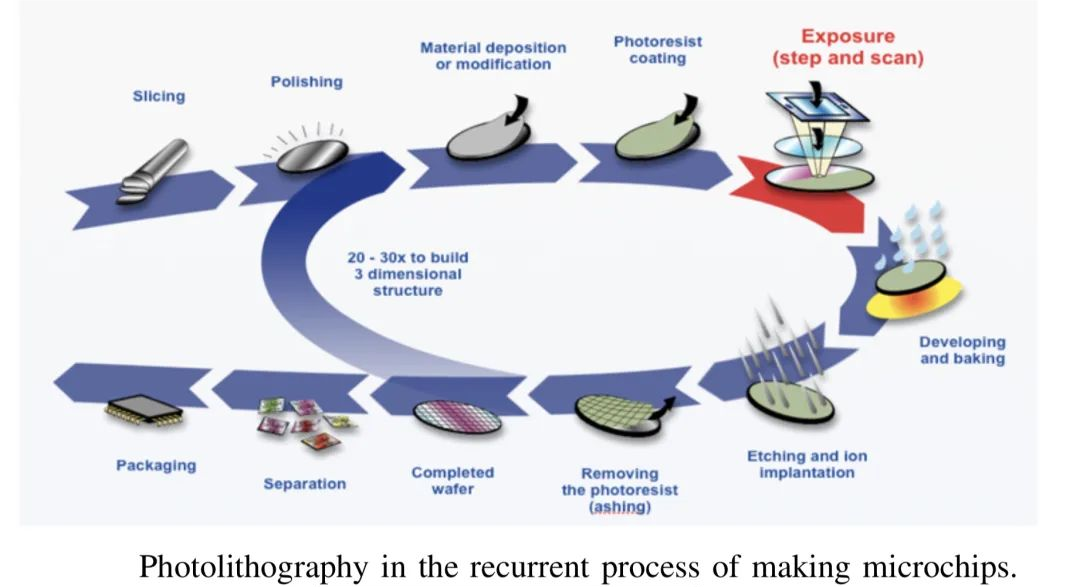
Wafer scanners utilize the principle of lithography, which is the patterning method for almost all integrated circuits manufactured today. [40] As such, it provides a key step in the circular process of manufacturing the microchip shown in Figure 1. Wafer scanner specifications are typically expressed in terms of overlay, resolution, focus, and throughput. Superposition, whether a single-machine superposition (SMO) or a matching machine superposition measured on the same system.
Light source: Light generation and control
The light source is a complex, non-linear, multiple-input multiple-output (MIMO) laser system. In this system, light is produced in the form of a train of pulses of a few kHz, called the repetition rate of the laser. The pulse train is followed by a quiescent state during which no light is produced, called the pulse train interval. It can be seen from (1) that the wavelength of the light source directly determines the size of the printable feature.
Optics: Isolation and control of vibration
The projection optical system is at the heart of the lithography tool as it forms an image of the original pattern on the mask onto the wafer. In DUV tools, the projection lens usually contains multiple refracting lens elements, while in EUV tools, multiple multilayer mirrors are used. In optical systems, there is usually a frame that serves as a position reference for optical elements and platforms. The optical element is either actively controlled relative to the frame or physically connected to it. In any case, the optical frame should be vibration-free in order to maintain a stable position of the optical element during operation. In addition, low frequency motion should be avoided to limit the deformation of the frame itself.
Platform:Part one - Motion control
Wafer and mask platform systems are fast and precise positioning systems for point-to-point movement (in series). In doing so, these systems rely heavily on control for tracking performance and interference suppression.
Stage: Part Two - Control of thermal deformation
Due to the exposure light produced by the light source, both the mask and the wafer will heat up and become partially deformed. This results in wafer level overlap and focusing errors. These problems are called mask heating and wafer heating respectively.
Outlook
The control of wafer scanners is expected to continue to benefit from theories and methods in the field of systems and controls. This involves linear and nonlinear theory, continuous and digital control, SISO and MIMO control, Kalman filtering, adaptive control, system identification, stochastic control, distributed parameter system control, and learning control. It is also involved in many fields of application, traditionally from various branches of physics such as classical mechanics, thermodynamics, electromagnetism and electronics, and optics. In addition, other fields such as mathematics and statistics also play an important role in statistical process control.
FOUNTYL TECHNOLOGIES PTE. LTD. was located in Singapore, we are focus on the research and development, manufacturing and technical services of precision ceramic parts in the semiconductor field for more than 10 years. our main product are ceramic vacuum chuck, ceramic end effector, ceramic plunger and ceramic beam&guide, and produces various of advanced ceramics (porous ceramics, alumina, zirconia, silicon nitride, silicon carbide, aluminum nitride and microwave dielectric ceramics) parts.