


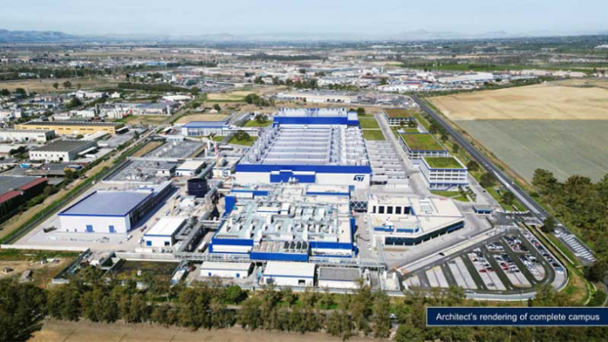
News

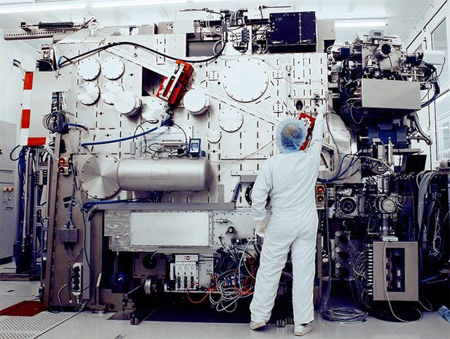
Principle and equipment of lithography machine
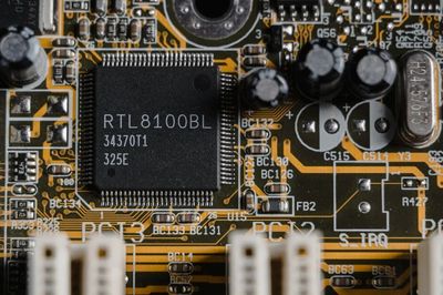
On the principle of lithography process, we can imagine the development of film photos, mask plate is equivalent to film, and the lithography machine is the development table, it copies the chip circuit on the mask plate to the photoresist film one by one, and then the circuit is "painted" on the wafer through etching technology.
Of course, the actual process is certainly not so simple, ASML's typical immersive step scan lithography machine as an example to see how the lithography machine is working - first of all, laser light, after correction, energy controller, beam forming device, etc., into the photomask desk, put on the design company's photomask, and then projected to the exposure desk through the objective lens. So what you have here is an 8-inch or 12-inch wafer, coated with a photoresist, which is photosensitive, and ultraviolet light etches circuits on the wafer.
The laser is responsible for the light source generation, and the light source is a decisive influence on the process process, with the continuous improvement of the semiconductor industry node, the wavelength of the lithographic laser is also constantly shrinking, from 436nm, 365nm near ultraviolet (NUV) laser into 246nm, 193nm deep ultraviolet (DUV) laser, At present, DUV lithography machine is a large number of applications of lithography machine, the wavelength is 193nm, the light source is ArF (argon fluoride) excimer laser, from 45nm to 10/7nm process can use this lithography machine, but to the 7nm node has the limit of DUV lithography, So Intel, Samsung and TSMC will introduce extreme ultraviolet (EUV) lithography technology at the 7nm node, and GlobalFoundries also studied the 7nm EUV process, but has now abandoned it. The lithography machine that uses extreme ultraviolet light (EUV) as a light source is an EUV lithography machine, of course, this is definitely not as simple as simply changing the light source.
Why is EUV lithography needed?
One of the advantages of EUV is the reduction of chip processing steps, and using EUV instead of traditional multiple exposure technology will greatly reduce the steps of deposition, etching, and measurement. At present, EUV technology is mainly used in logical process processes, which has led to an increase in order volume/demand in 2019.
The 193nm light source DUV used today has actually been used since the 2000s, but it is stuck in the technology of more short-wavelength light sources, and the lithography technology of 157nm wavelength has actually had a lithography machine in 2003, but the progress compared to the 193nm wavelength is only 25%. However, because the 157nm light wave will be absorbed by the 193nm lens, the lens and the photoresist have to be re-developed, and the cheaper immersion 193nm technology has been available at that time, so the 193nm DUV lithography has been used now.
Of course, we must want to know why the same light source can be derived from so many different process nodes, taking Intel as an example, in 2000, 180nm was used, and now it is 10nm, in fact, the lithography machine determines the semiconductor process process, the accuracy of the lithography machine is related to the wavelength of the light source and the numerical aperture of the objective lens. There are formulas to calculate:
(process ∝1/) lithography machine resolution =k1*λ/NA (k1 is a constant, different lithography machine k1 is different, λ refers to the wavelength of the light source, NA is the numerical aperture of the objective lens, so the resolution of the lithography machine depends on the wavelength of the light source and the numerical aperture of the objective lens, the shorter the wavelength, the larger the NA, the better, so the higher the resolution of the lithography machine, The more advanced the process technology.) (Note: The blue part of the formula is added according to the above formula description, so it is logical)
The original immersion lithography is very simple to add 1mm thick water on the wafer resist, water can refract the light wavelength of 193nm into 134nm. Later, continuous improvement of high NA lenses, multi-light, FinFET, Pitch-split and band Suzuki photoresist technology, one only used the current 7nm/10nm, but this is the limit of the 193nm lithography machine. In the existing technical conditions, NA numerical aperture is not easy to improve, the NA value of the lens currently used is 0.33, you may remember that there was a news before, that is, ASML invested 2 billion US dollars in Carl Zeiss, the two sides will cooperate to develop a new EUV lithography machine, many people do not know what relationship EUV lithography machine has with Zeiss. Now it should be understood that ASML and Zeiss cooperation is to develop NA 0.5 optical lenses, which is the key to further improve the resolution of EUV lithography machine in the future, but the high NA EUV lithography machine is at least 2025-2030, it is still far away, and the progress of optical lenses is much more difficult than electronic products. The NA value can not be improved for a time, so the lithography machine chose to change the light source, replacing the 193nm DUV light source with 13.5nm wavelength EUV, which can also greatly improve the resolution of the lithography machine.
In the second half of the 1990s, everyone was looking for a technology to replace the 193nm lithography light source, and proposed including 157nm light source, electron beam projection, ion projection, X-ray and EUV, and from the current results, only EUV is successful. At the beginning, led by Intel and the US Department of Energy, the collection of MOTOROLA, AMD and other companies and the three national laboratories in the United States formed EUV LLC, and ASML was also invited to become a member of EUV LLC. Between 1997 and 2003, several hundred scientists at EUV LLC published numerous papers demonstrating the feasibility of EUV lithography, and then EUV LLC was dissolved.
The world's first EUV lithography machine prototype in 2006
Next ASML launched the prototype of the EUV lithography machine in 2006, built a 10,000 square meters of clean studio in 2007, created the first research and development prototype NXE3100 in 2010, and finally created a mass-produced prototype in 2015, and in this research and development process, Intel, Samsung, TSMC, these semiconductor manufacturers blood transfusion is absolutely a lot.
As the only manufacturer in the world capable of EUV lithography, ASML naturally obtained a large number of orders, as of the second quarter of 2019, ASML's NEX:3400B EUV lithography machine installed number has reached 38, and in the second half of the year they launched the more efficient NEX:3400C lithography machine. In the whole year of 2019, a total of 26 sets of EUV lithography machines were delivered, which brought them a revenue of 2.789 billion euros, accounting for 31% of the annual revenue, and the ArFi far-ultraviolet lithography machine that sold 82 units in the whole year earned 4.767 billion euros, which shows how much money a set of EUV lithography machine is. The new NEX:3400C has increased its production capacity from 125 wafers per hour to 170 wafers per hour, and sales have increased significantly.
Although the EUV lithography machine is quite expensive, close to $120 million a piece, but semiconductor manufacturers are willing to invest, because 7nm and above processes do need EUV lithography machine, when the same 7nm process, the use of EUV lithography technology after the transistor density and performance are better, according to TSMC data, compared with the original 7nm process, The 7nm EUV (N7+) can provide a 1.2-fold increase in density, a 10% increase in performance for the same power consumption level, or a 15% power savings for the same performance.
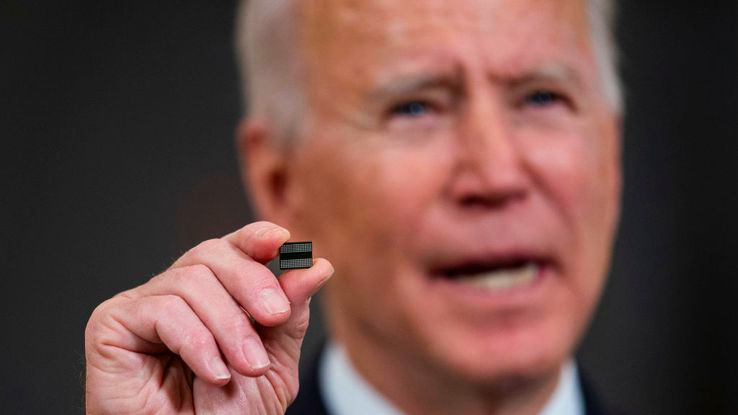
Now Samsung and TSMC have used the 7nm EUV process to start the production of chips, the AMD Zen 3 architecture fourth generation Rydragon processor scheduled to be released this year is TSMC 7nm EUV process, Intel's current 10nm process has not yet used EUV technology, but it is scheduled to use EUV lithography in the 7nm process period. The domestic SMIC also ordered an EUV lithography machine from ASML, but due to various problems, the delivery time is not yet clear.
Fountyl Technologies PTE Ltd, is focusing on semiconductor manufacturing industry, main products include: Pin chuck, porous ceramic chuck, ceramic end effector, ceramic square beam, ceramic spindle, welcome to contact and negotiation!