


News


Silicon carbide ceramics: increasingly indispensable precision component materials in semiconductor manufacturing processes
As a structural ceramic material with excellent performance, silicon carbide (SiC) has the characteristics of high density, high thermal conductivity, high bending strength, high elastic modulus, strong corrosion resistance, high temperature resistance, etc. It is not easy to produce bending stress deformation and thermal strain, and can adapt to the strong corrosion and ultra-high temperature reaction environment of wafer epitaxy, etching and other manufacturing links. Therefore, it has been widely used in semiconductor manufacturing processes such as grinding and polishing, epitaxial/oxidation/diffusion heat treatment, lithography, deposition, etching, and ion implantation.
Grinding process
When the ingot is cut into a wafer, it usually forms a sharp edge, with edges, burrs, chipping, small cracks or other defects. In order to avoid the influence of edge cracking on the wafer strength, damage to the wafer surface finish, and bring pollution particles to the post-process, the wafer needs to be polished by grinding process, reduce the thickness of the wafer, improve the parallelism of the wafer surface, and eliminate the surface damage caused by the wire cutting process. At present, the most commonly used method is to use the grinding disc for double-sided grinding, and to improve the quality of the grinding disc by improving the grinding process (grinding disc material, grinding pressure and grinding speed, etc.).
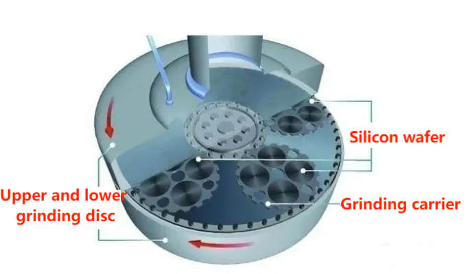
In the past, the grinding disc is mostly used in cast iron or carbon steel materials, which has a short service life and a large coefficient of thermal expansion. In the process of processing silicon wafers, especially when high-speed grinding or polishing, the flatness and parallelism of silicon wafers are difficult to ensure due to the wear and thermal deformation of the grinding disc. With the development of silicon carbide ceramic wear-resistant materials and the development of sintering process, cast iron and carbon steel grinding disc is gradually replaced by silicon carbide grinding disc, its high hardness, low wear characteristics and with silicon wafer basically the same thermal expansion coefficient, the application in high-speed grinding polishing process has outstanding advantages.
Heat treatment and other processes
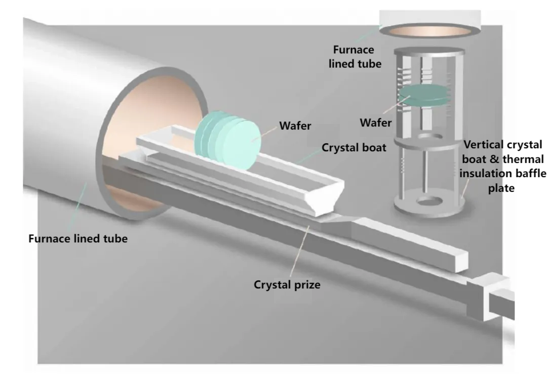
Wafer manufacturing can not be separated from oxidation, diffusion, annealing, alloy and other heat treatment processes, mainly involved in silicon carbide ceramic products including silicon carbide ceramic arms used to transport wafers between processes and parts in the reaction chamber of heat treatment equipment.
· Ceramic arm
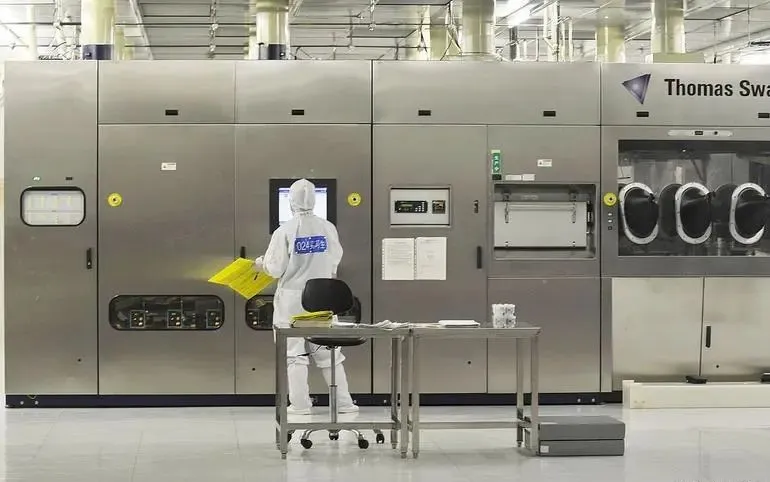
In the production of silicon wafers, it is necessary to undergo high temperature heat treatment, and a mechanical arm is often used to move, transport and position semiconductor wafers. Because semiconductor wafers are required to be clean and fast in the handling process, and most processes are carried out in vacuum, high temperature and corrosive gas environment, they need to have high mechanical strength, corrosion resistance, high temperature resistance, wear resistance, high hardness, insulation and so on. Compared with alumina, silicon carbide ceramic arm can better meet these requirements, but the shortcomings of high price and difficult processing restrict its application to a certain extent.
· Components in the reaction chamber
The semiconductor equipment used in the heat treatment process has oxidation furnaces (which are divided into horizontal furnaces and vertical furnaces), rapid heat treatment (RTP, RapidThermalProcessing) equipment, etc. Due to the high operating temperature, the performance requirements of the components in the reaction chamber are also high. High-purity sintered silicon carbide parts have the characteristics of high strength, high hardness, high elastic modulus, high specific stiffness, high thermal conductivity, low thermal expansion coefficient, etc., and are indispensable parts in the reaction chamber of integrated circuit heat treatment equipment. It mainly includes vertical boat (VerticalBoat), Pedestal (Pedestal), LinerTubes (LinerTubes), inner tubes (InnerTubes) and heat insulation BafflePlates.
At present, most of the market share of high-purity sintered silicon carbide market for semiconductor equipment is mainly dominated by foreign companies such as Japan Kyokera Group and the United States Quastai. Through long-term technological accumulation and innovation, they have developed not only a complete range of products, but also the processing technology of material properties, precision and complex structure has reached the industry leading level. It can provide special components for integrated circuit core equipment such as photolithography machine, plasma etching equipment, film deposition equipment and ion implantation equipment. In contrast, China started late in the research and development and application of sintered silicon carbide parts for semiconductor equipment, and still faces technical bottlenecks and challenges in the field of preparation of sintered silicon carbide parts with high precision, large size, lightweight and special structures (such as hollow, closed cell).
Light engraving process
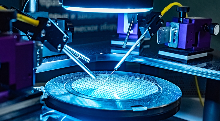
Photolithography mainly uses an optical system to focus the light beam emitted by the light source and project it onto the silicon wafer to achieve exposure of the circuit pattern and facilitate subsequent etching, whose accuracy directly determines the performance and yield of the integrated circuit. As one of the top equipment for chip manufacturing, the lithography machine contains up to 100,000 parts, and in order to ensure the performance and accuracy of the circuit, both the optical components and the precision of the components in the lithography system have extremely high requirements. The application of silicon carbide ceramics mainly includes: workpiece table, ceramic square mirror and so on.
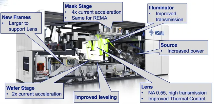
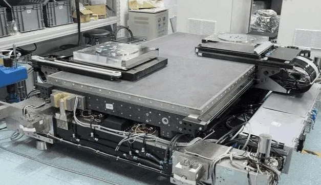
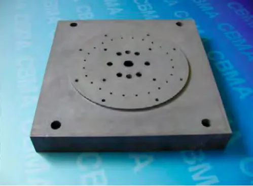
· Workpiece table
The lithographic machine table mainly carries the wafer and completes the exposure movement. In this process, the silicon wafer and the workpiece table need to be aligned before each exposure, and then the light mask and the workpiece table are aligned to achieve the alignment of the light mask and the silicon wafer, so that the graphics are accurately copied to the area that needs to be lithographed, which requires the workpiece table to achieve high-speed, smooth, and high motion precision nanoscale ultra-precision automatic control. In order to achieve this control purpose, the lithographic workpiece table is generally used with light weight and extremely high dimensional stability, low thermal expansion coefficient, and is not easy to produce deformation, in order to reduce the motion inertia, reduce the motor load, and improve the motion efficiency, positioning accuracy and stability.
· Ceramic square mirror
One of the key technologies of the lithography machine is the synchronous motion control of the workpiece table and the mask table, the precision of which directly affects the lithography accuracy and yield of the lithography machine. The measuring system first uses the interferometer to send out the measuring beam incident on the square mirror on the side of the workpiece table, and then reflects it back to the receiver of the interferometer. The position change of the workpiece table is calculated by Doppler principle and fed back to the motion control system in real time to ensure the synchronous movement of the workpiece table and the mask table. Silicon carbide ceramics have the characteristics of lightweight, can meet the requirements of the use of ceramic square mirror, but the preparation of such silicon carbide ceramic parts is more difficult, the current international mainstream integrated circuit equipment manufacturers mainly use glass-ceramics, cordierite and other materials. However, with the progress of technology, experts from the China General Institute of Building Materials Science and Research have realized the preparation of large-size, complex shape, highly lightweight, fully enclosed silicon carbide ceramic square mirrors and other structural and functional optical components for lithography machines.
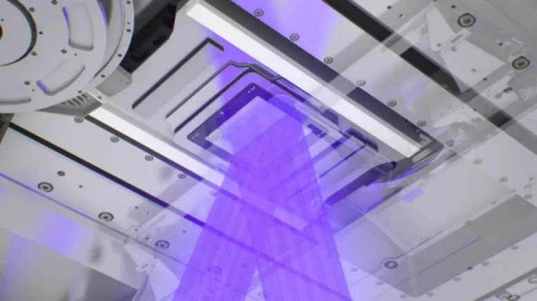
· Light mask film
The light mask is also known as the light mask, the main role is to transmit light through the mask and form a pattern on the photosensitive material. However, when the EUV light shines on the mask, it will emit heat, and the temperature may rise to between 600 and 1,000 degrees Celsius, which may cause thermal damage. Therefore, it is usually necessary to deposit a silicon carbide film on the light. At present, many foreign companies, such as ASML, have begun to supply films with light transmittance of more than 90% to reduce the cleaning and inspection of the mask in use, and to improve the efficiency and product yield of EUV lithography machines.
Plasma etching and deposition
The etching process in semiconductor manufacturing uses plasma ionized by liquid or gaseous etchers (such as fluorinated gases) to bombard the wafer, selectively removing unwanted materials until the desired circuit pattern is left on the wafer surface. Thin film deposition is similar to the reverse process of etching, which uses the method of deposition to repeatedly stack insulating materials and cover each layer of metal to form a thin film. Since these two processes also use plasma technology and other technologies that are easy to cause corrosion to the cavity and components, the components in the equipment are required to have good plasma resistance characteristics and low reactivity and low conductivity to fluorine-containing etched gases.
Traditional etching and deposition equipment components, such as focusing rings, are made of materials such as silicon or quartz. However, with the advancement of integrated circuit miniaturization, the demand and importance of integrated circuit manufacturing for etching process is increasing, and it is necessary to use high-energy plasma to precisely etch silicon wafers at the microscopic level, which provides the possibility to achieve smaller line widths and more complex equipment structures. Therefore, chemical vapor deposition (CVD) silicon carbide with its excellent physical and chemical properties. And high purity, high uniformity and so on have gradually become the first choice of etching, deposition equipment coating materials. At present, CVD silicon carbide parts in etching equipment include focusing rings, gas spray heads, pallets, edge rings, etc. In the deposition equipment, there are chamber cover, cavity lining, SiC coated graphite base, etc.
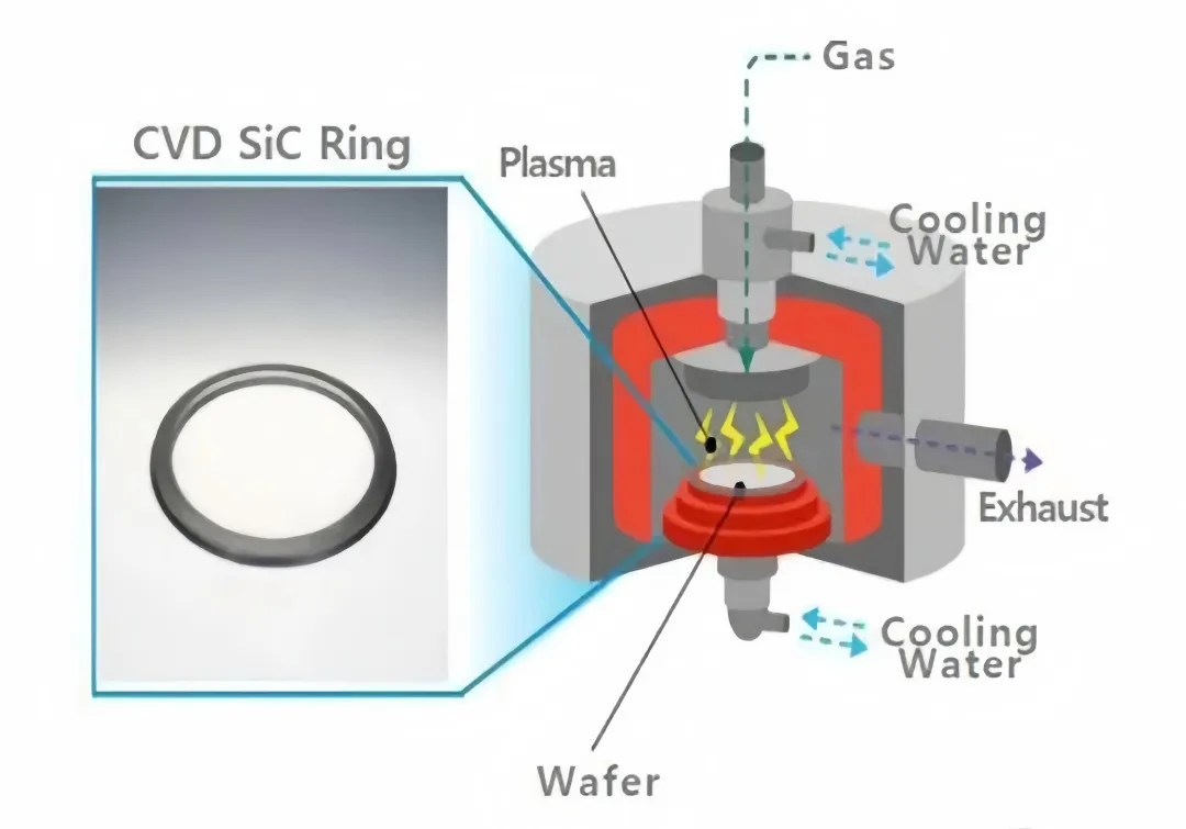
Due to the low reactivity and conductivity of CVD silicon carbide to chlorine and fluorine etching gases, it is an ideal material for focusing rings and other components of plasma etching equipment. The CVD silicon carbide parts in the etching equipment include focusing ring, gas spray head, pallet, edge ring, etc. Taking the focus ring as an example, the focus ring is an important part placed on the outside of the wafer, directly in contact with the wafer, by applying a voltage to the ring to focus the plasma passing through the ring, thereby focusing the plasma on the wafer to improve the uniformity of processing. Traditional focusing rings are made of silicon or quartz. With the advancement of integrated circuit miniaturization, the demand and importance of integrated circuit manufacturing for etching process is increasing, and the power and energy of etching plasma continue to increase, especially the plasma energy required in capacitive coupled (CCP) plasma etching equipment is higher. Therefore, the use rate of focusing rings prepared by silicon carbide materials is getting higher and higher.
Fountyl Technologies PTE Ltd, is focusing on semiconductor manufacturing industry, main products include: Pin chuck, porous ceramic chuck, ceramic end effector, ceramic square beam, ceramic spindle, welcome to contact and negotiation!