


Industry News


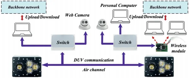
The use of deep ultraviolet light to advance the development of communications
The use of deep ultraviolet light for wireless optical communication is very attractive.
Us announces 3D semiconductor roadmap
SEMICONDUCTOR RESEARCH CORPORATION (SRC) has unveiled its Microelectronics and Advanced Packaging (MAPT) roadmap, developed by a collaborative effort of about 300 individuals from 112 organizations in industry, academia and government.
Control of Wafer Scanners: Methods and Developments
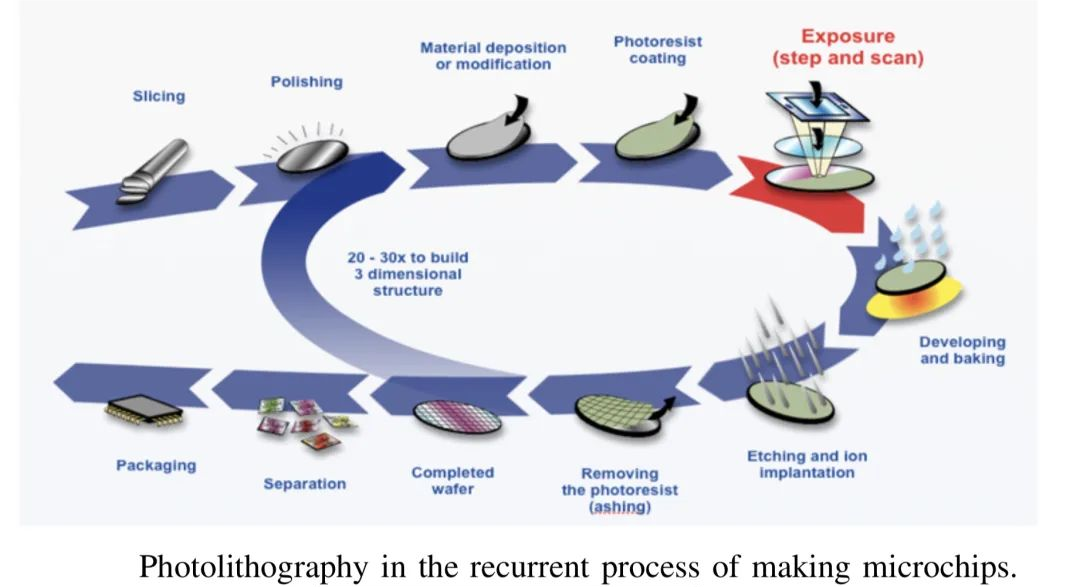
Today's information economy, including paradigms such as the Internet of Things and the era of big Data, is built on half a century of technological developments in the semiconductor industry based on Moore's Law. The main technological enabler behind these developments is widely believed to be the lithography process.
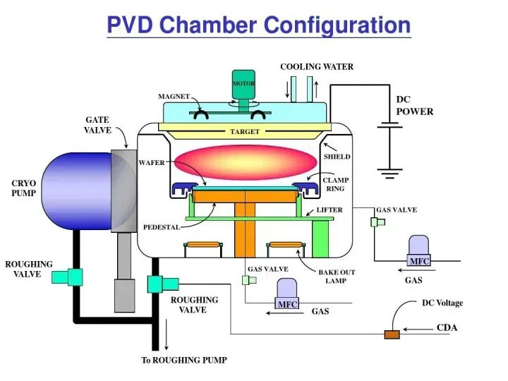
Ten kinds of deposition technologies about PVD & PVD and CVD & AMAT PVD product Introduction
With the development of technology, PVD technology is also constantly innovating, there are a lot of specialized technologies for certain uses, in this special inventory for everyone to introduce a variety of PVD technology.

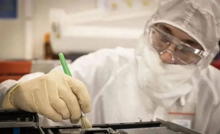
Wafer cleaning Clean/Wet equipment market analysis
The entire semiconductor process needs to be repeatedly cleaned, and the cleaning process runs through the semiconductor industry, accounting for more than 30% of the total production process.
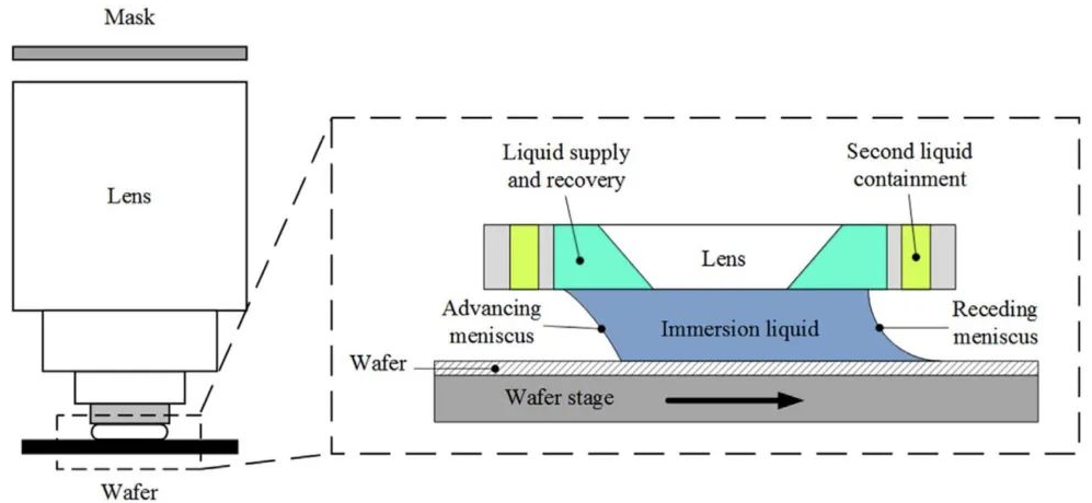
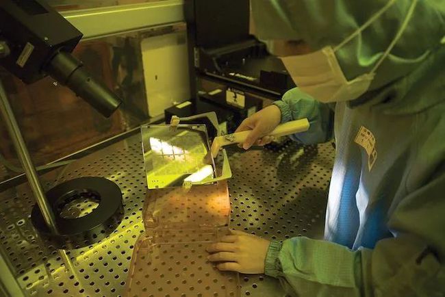
Flow control in immersion lithography
For more than ten years, immersion lithography has been the main exposure technology in semiconductor manufacturing.
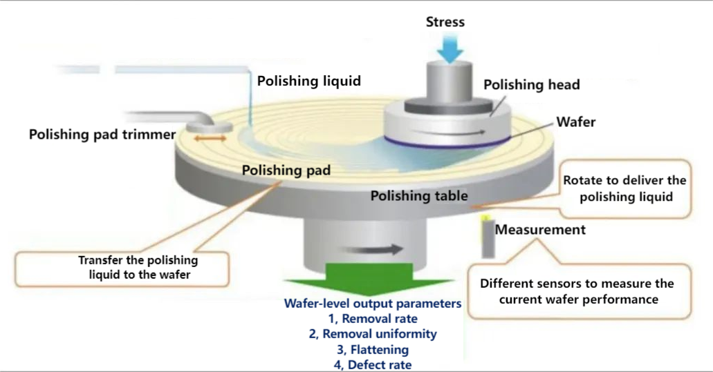
CMP chemical mechanical polishing equipment principle and the introduction of domestic and foreign equipment manufacturers
Chemical mechanical polishing (CMP) is a technique used in the fabrication of integrated circuit chips to achieve wafer surface flatness
Silicon carbide ceramics: increasingly indispensable precision component materials in semiconductor manufacturing processes
Semiconductor manufacturing is the cornerstone of the development of modern science and technology, with the industry's continuous pursuit of smaller, faster, more efficient integrated circuits, the precision and technical complexity of the manufacturing process is also increasing, every step is inseparable from high-performance, high-quality and high-precision semiconductor equipment.