


News


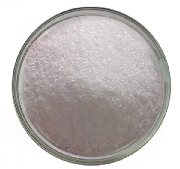
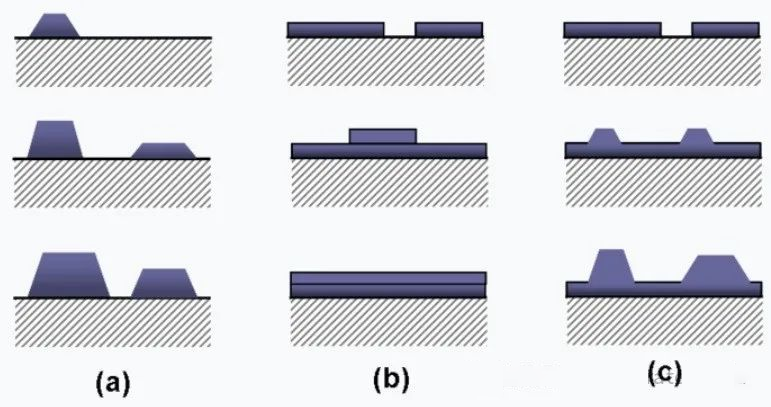
Special ceramics: Press molding - binder
Organic binders are often used in dry pressing and isostatic pressing.
Ceramic parts & Quartz Parts & perfluorinated Seals & Electrostatic chuck....
At present, domestic vacuum semiconductor parts are equivalent to the development stage of domestic semiconductor equipment about 3 to 5 years ago, and several domestic suppliers of various parts and components continue to research and development, but are limited by the technology gap has not fully met the needs of downstream semiconductor equipment manufacturers
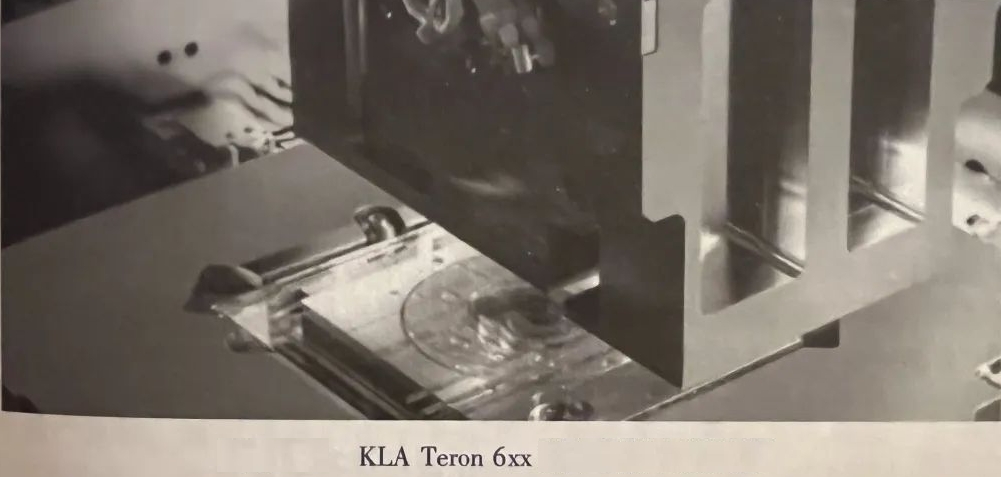
Domestic and foreign testing equipment leading enterprises and equipment introduction
Domestic and foreign testing equipment leading enterprises and equipment introduction

Infrared Optical Design Talk! Material or big problem!
Infrared optical system in the design process may feel that the difficulty is relatively low, a conventional objective lens may be three mirrors to get it done, this is a relatively entry-level design, complex and infrared zoom, multi-channel composite system.
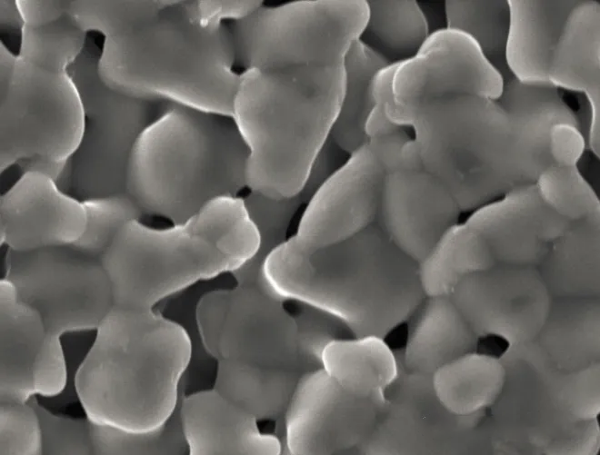
Sintering of ceramics -- mechanism and method of sintering
Sintering is an important process in powder metallurgy, ceramics and refractory materials
What is epitaxy?
Epitaxy refers to a crystal growth or material deposition technology that occupies an extremely important position in microelectronics and optoelectronics manufacturing processes
What is the difference between substrate and epitaxy?
In the semiconductor industry chain, especially in the third generation semiconductor (wide band gap semiconductor) industry chain, there will be a substrate and epitaxial layer, what is the significance of the existence of epitaxial layer? What's the difference from the substrate?
Semiconductor equipment industry in-depth review
Semiconductor equipment is the cornerstone to support the development of the electronics industry, but also the semiconductor industry chain upstream market space is the broadest, the most important strategic value of a link.
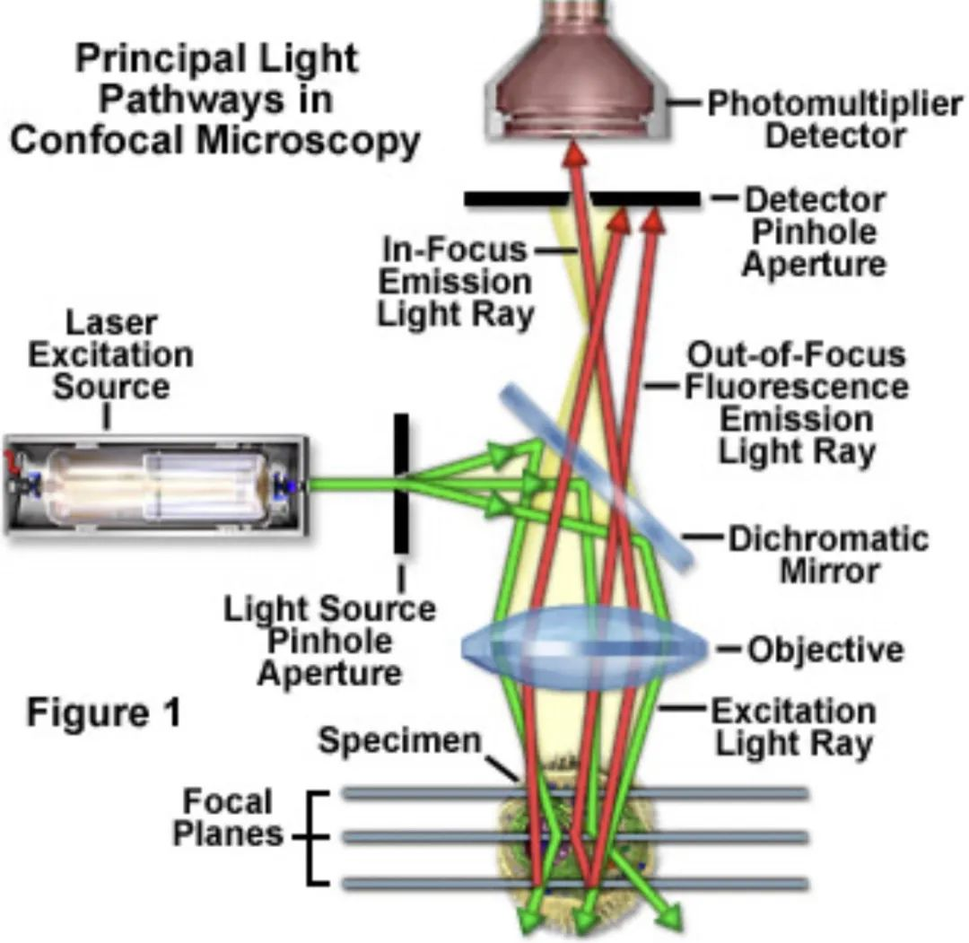
Confocal light microscope
The laser is focused on the wafer, illuminates a light spot, and the reflected light is refocused on the receiving plane, and through the analysis of the light, the surface of the silicon wafer is detected. The microscope is a system in which laser light is focused on a silicon chip and the reflected light is designed to be focused using a receiver
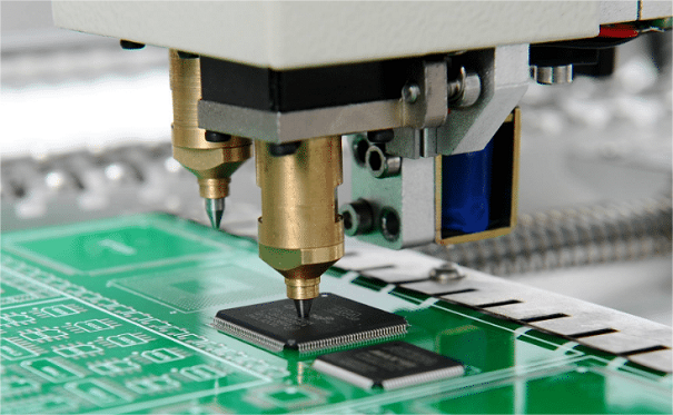
Chip bonding: The process of placing a chip on a substrate
The packaging process is the last step in the manufacturing of semiconductors, and its sequence is grinding, cutting, mounting, wiring, and forming. The sequence of these processes can change according to the changes in packaging technology, and can also be closely related to each other or combined