


News


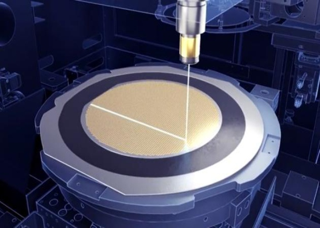
Silicon carbide wafer cutting types
Silicon carbide (SiC) is considered as an alternative material for silicon (Si) -based semiconductors in the electronics industry due to its wide band gap, high mechanical strength and high thermal conductivity. SiC power devices caoperate at higher voltages, frequencies, and temperatures, and are able to convert power with higher efficiency or lower power losses.
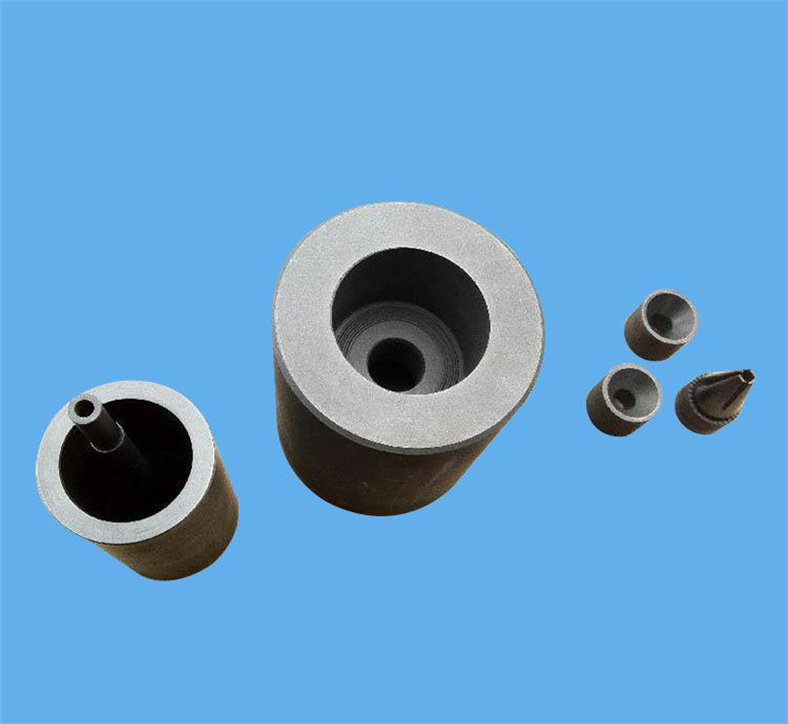
High purity graphite - a key consumable in the third generation semiconductor field
High purity graphite has high temperature resistance, good electrical conductivity and chemical stability, and has become a key material in the semiconductor field.
In the first quarter of 2024, 144 tech companies laid off nearly 35,000 employees.
On February 19, Cisco said it would cut 5% of its global workforce, more than 4,000 working post , and lower its annual revenue target because of tough economic conditions.
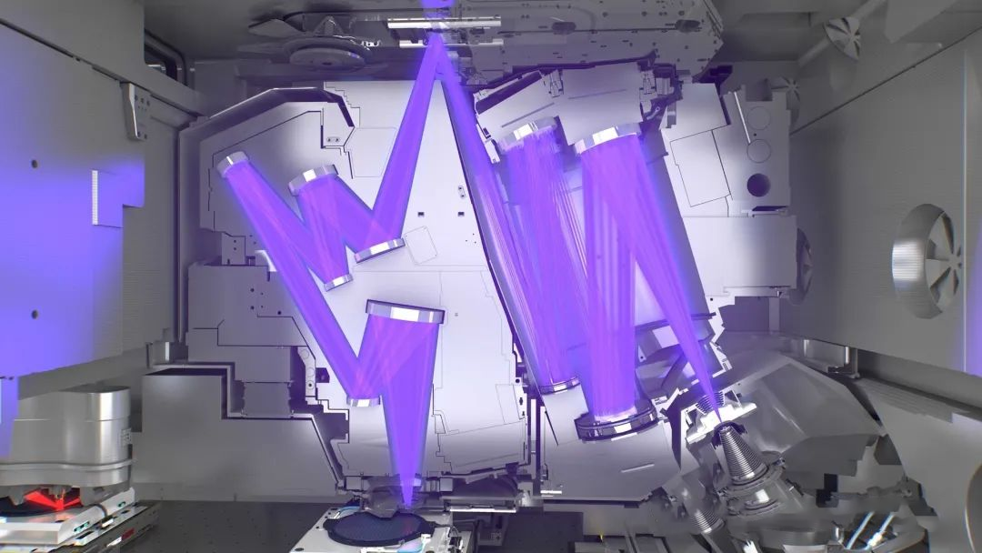
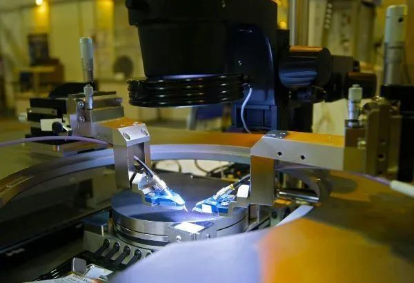
Precision silicon carbide ceramic components for lithography machines
The key technologies and equipment of integrated circuit manufacturing mainly include lithography technology and lithography equipment, film growth technology and equipment, chemical mechanical polishing technology and equipment, high-density post-packaging technology and equipment, all involve motion control technology and drive technology with high efficiency, high precision and high stability. The accuracy of structural parts and the performance of structural materials have very high requirements.
Introduction of aluminum nitride ceramic heater, a key component of semiconductor equipment
In the wafer manufacturing process, the wafer needs to be heated to a certain temperature, and the wafer temperature uniformity has a very strict requirement, because the wafer temperature uniformity has a very important impact on the quality of semiconductor chips; At the same time, it is also necessary to work in vacuum, plasma, chemical gas environments, which requires the use of ceramic heaters.
Introduction on application of semiconductor precision ceramics
Semiconductor chips are everywhere, equivalent to the brain of electronic products, mobile phones, smart watches, computers, cars, big data, cloud computing, the Internet of things are upgraded can not be separated from it. In the semiconductor industry, advanced ceramics are the foundation of the entire semiconductor industry foundation.
The latest technology! Intel announced 3D chip technology, logic unit, back power supply of future foundry technology at IFS Direct Connect conference!
Recently an exclusive interview ahead of an invitation-only event in SAN Jose, Intel outlined the new chip technologies it will offer its contract customers by sharing a glimpse of its future data center processors.
Samsung divest ASML with profit by 8 times, why will the interest groups linked to EUV lithography machines be disintegrated?
In the field of wafer foundry, TSMC has always been the industry leader, and Samsung is the second largest in the industry, but the gap between the second and the oldest is very large, TSMC's share is as high as 58.5%, and Samsung's share is only 15.8%.
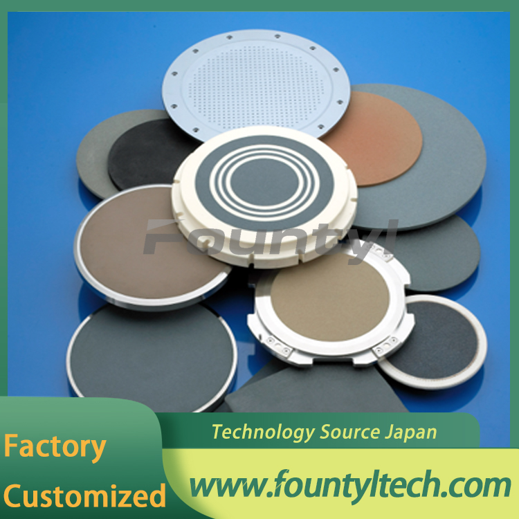
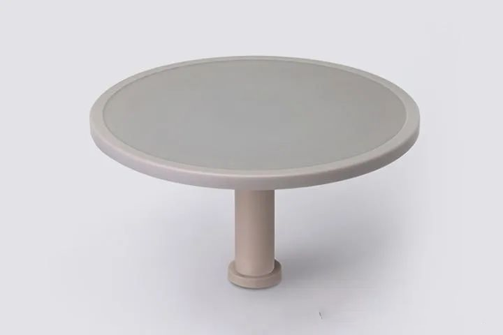
Singapore porous ceramic chuck table, Southeast Asia precision porous ceramic parts vacuum chuck
The pore size of the special porous ceramic material is 2 ~ 3 microns, and it is difficult to plug with large vacuum force and partial area adsorption. It can also be used as an air floating platform, which is widely used in semiconductor, panel, laser processing and non-contact linear slider fields. Porous ceramic vacuum chuck maintain transmission by sealing air. The application of the device is limited to the flat, non-porous surface of the working platform. The user is usually the machine operator.
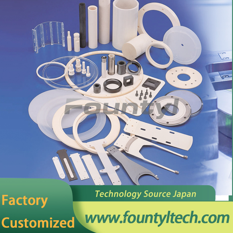
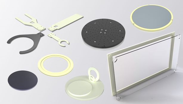
Semiconductor ceramics - custom manufacturing
Fountyl Technologies PTE Ltd is an industry leading ceramic manufacturer of wafer processing equipment technology, and we are constantly optimizing and upgrading the manufacturing process of semiconductor ceramics to achieve better product quality and improve the durability of our products: high aluminum ceramic arms, robotic end effectors, ceramic wafer chucks, wafer handling and machining parts, and custom products. Please consult us directly for detailed dimensions and tolerances