


News


Silicon carbide ceramics: increasingly indispensable precision component materials in semiconductor manufacturing processes
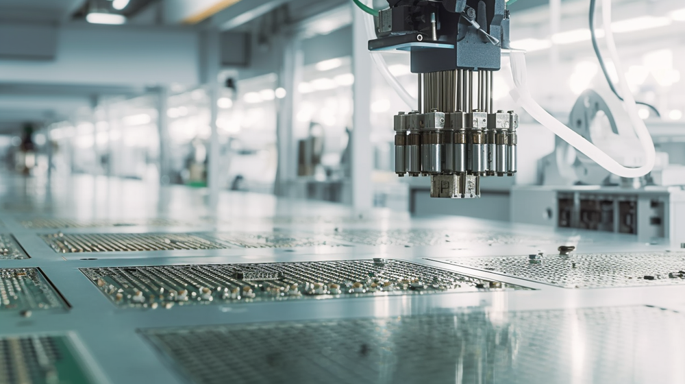
Semiconductor manufacturing is the cornerstone of the development of modern science and technology, with the industry's continuous pursuit of smaller, faster, more efficient integrated circuits, the precision and technical complexity of the manufacturing process is also increasing, every step is inseparable from high-performance, high-quality and high-precision semiconductor equipment.
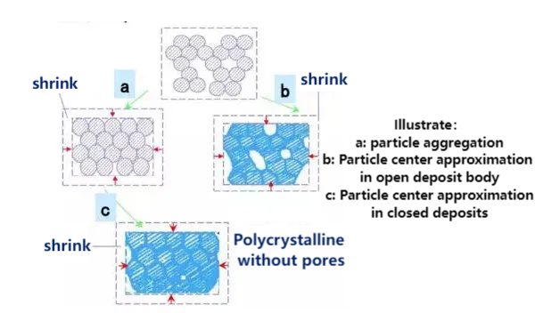
Process verification of special ceramics research and development
Technology (craft) refers to the method and process by which workers use various production tools to process or treat various raw materials and semi-finished products, and finally make them into finished products.
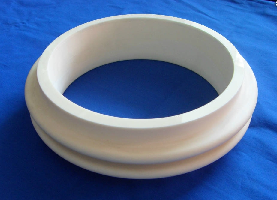
Silicon carbide ceramics used in semiconductor/integrated circuit manufacturing equipment
Silicon carbide ceramics play an important role in semiconductor/integrated circuit manufacturing equipment due to their unique physical and chemical properties.

Semiconductor equipment manufacturers, up 111%!
On May 9, Japanese semiconductor manufacturing equipment manufacturer Screen Holdings announced the 2023 fiscal year (April 2023 - March 2024) financial results, revenue and profit have set a new record, and 2024 annual performance is expected to continue to hit a new high.
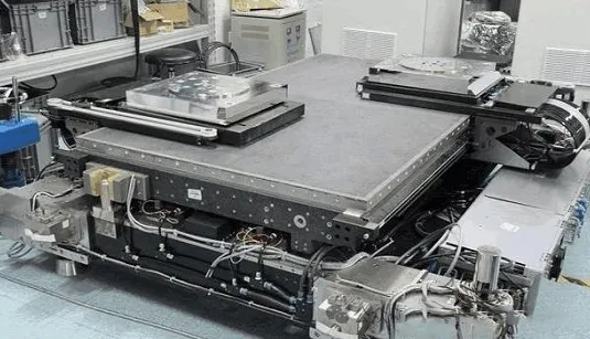
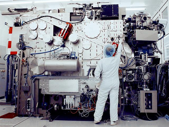
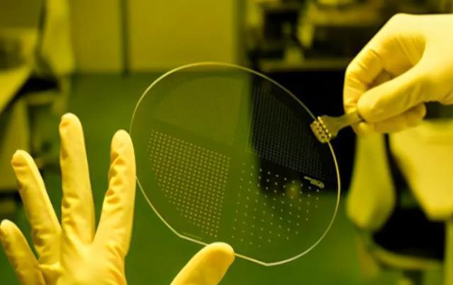
How to understand semiconductor manufacturing equipment
Semiconductor manufacturing process is the process of processing silicon wafers into semiconductor chips. It can be roughly divided into front segment and back segment.
Development and application of alumina ceramics
Alumina ceramics have high mechanical strength, large insulation resistance, high hardness, wear resistance, corrosion resistance and high temperature resistance and a series of excellent properties, which are widely used in ceramics, textile, petroleum, chemical, construction and electronics and other industries.
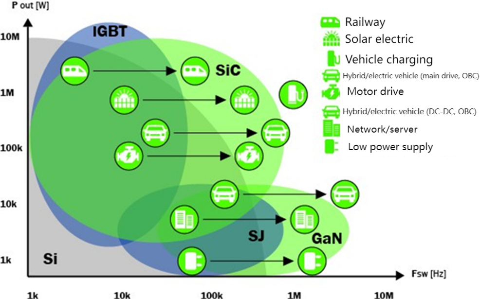
What is the difference between gallium nitride (GaN) and silicon carbide (SiC)?
Silicon has dominated the transistor world for decades. But that is changing. Compound semiconductors consisting of two or three materials have been developed that offer unique advantages and superior properties.
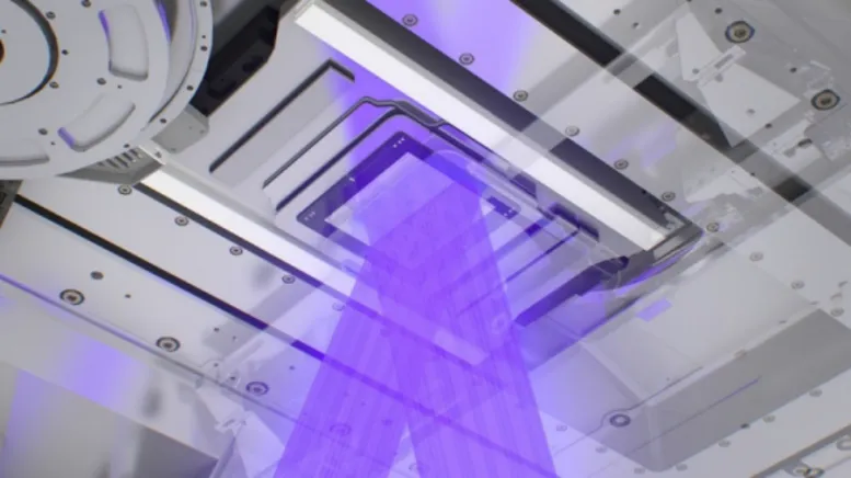
Principle and equipment of lithography machine
One of the advantages of EUV is the reduction of chip processing steps, and using EUV instead of traditional multiple exposure technology will greatly reduce the steps of deposition, etching, and measurement
Japanese companies monopolize the EUV photoresist supply market
Although there will be more photoresist manufacturers for EUV lithography. But at the moment the market is dominated by Japanese companies.
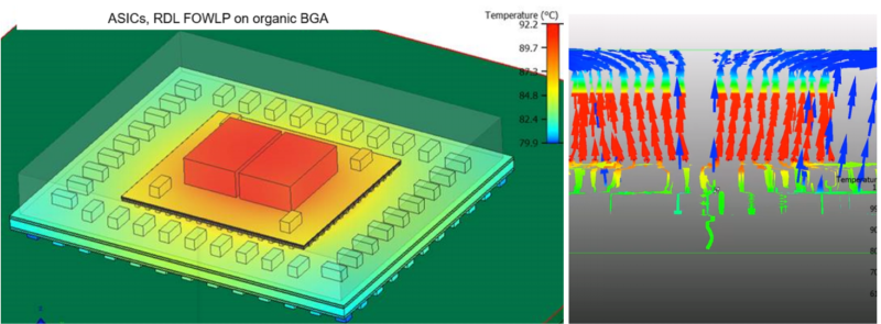
How to solve the chip package heat dissipation problem
Placing multiple chips side-by-side in the same package can mitigate thermal issues, but as companies delve further into chip stacking and denser packages to improve performance and reduce power, they're battling a new set of heat-related issues.