


News


Ceramic electrostatic chuck: How is this "stuck neck" semiconductor component produced?
From the PC+ Internet era to the mobile + social media era, and then to the future AI+ big data era, in order to meet the growing and diversified trend of system demand, wafer-level packaging technology is constantly breaking through in the direction of high-density, ultra-thin, ultra-small and higher performance, and at the same time, the clamping problem of ultra-thin device wafers has also put forward new demands and challenges.
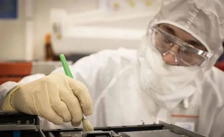
Traditional wafer clamping methods include mechanical clamping, paraffin bonding and other methods often used in the traditional machinery industry, which are easy to cause damage to the wafer, and it is easy to warp the wafer and pollute the wafer, which has a great impact on its processing accuracy. Later, vacuum chuck prepared by porous ceramics were gradually developed. Because the vacuum chuck is the use of silicon and ceramic surface to form negative pressure and absorb the wafer, easy to cause local deformation of the wafer and affect the flatness, so in recent years, with a stable and uniform adsorption force, will not pollute the wafer and can effectively control the temperature of the wafer ceramic electrostatic chuck has gradually become an ideal clamping tool for ultra-thin wafers.
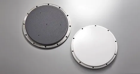
How do electrostatic chuck work? In general, ceramic electrostatic chuck is mainly composed of dielectric adsorption layer, electrode layer and base layer, which are stacked from the surface to the inside in a layered structure, and the dielectric adsorption layer is located on the surface to achieve efficient adsorption. The electrode layer is located in the middle, by adding a positive or negative voltage, forming an electrostatic field, and the base layer plays a supporting and fixing role. In addition, the electrostatic sucker can also be embedded in the electrode column, gas channel, bonding material and other auxiliary structures, wherein the gas can be passed into He gas during work, through the gas circulation flow for heat transfer, so as to stabilize the temperature of the wafer.
According to whether the dielectric adsorption layer is a doped dielectric, electrostatic chuck can be divided into Coulomb class and rotary hot back (JR) class, the suction cups made of pure dielectric (high impedance ceramic materials) are Coulomb class, and the suction cups made of doped dielectric (such as doped titanium oxide (TO2) and other substances, belong to the semiconductor) are rotary rotary hot back (JR) class. The adsorption principle of the two is very different, both are the use of DC power supply, the electrostatic field formed in the electrode layer, so that the surface of the dielectric layer produces a charge with the opposite polarity of the surface charge of the wafer, and the wafer adsorption. However, because the dielectric has a certain conductivity, in addition to the polarization charge, there is a large part of the free charge, so the suction force of the JR type suction cup is larger than that of the Coulomb type suction cup, and the adsorption can be achieved under a small voltage, but in the desorption stage, due to the free charge on the surface of the JR type suction cup, in addition to turning off the high voltage DC power supply, It is usually necessary to use a reverse static voltage to force the removal of residual charge before the chip can desorption, which increases the difficulty and complexity of control to a certain extent.
How are electrostatic chuck produced?
01 Material selection
Compared with metal materials, ceramic materials are not only wear-resistant, avoid the risk of chip pollution, but also have inherent advantages in electrical insulation, so electrostatic chuck technology is mainly based on alumina ceramics or aluminum nitride ceramics as the main material. In general, for ordinary silicon wafer processing, the use of high-purity aluminum oxide as a material can meet the needs, but for silicon carbide wafer processing, you need to use aluminum nitride electrostatic chuck.
Aluminum nitride thermal conductivity (theoretically up to 320W/(m·K)), matching coefficient of thermal expansion with electrode materials, insulation and related mechanical properties are better than alumina, not only can be in the plasma halogen vacuum environment can be sustained operation, withstand the semiconductor and microelectronics the most demanding process environment, but also by controlling its volume resistivity, Providing more stable and sufficient adsorption force and better temperature control, it is expected to gradually replace the electrostatic chuck of alumina ceramics, which is the main development direction of electrostatic chuck in the future. However, in the preparation process, due to the higher melting point of aluminum nitride, atomic self-diffusion coefficient is small, so pure AlN ceramics are difficult to sintering densification, often need to sintering temperature up to 1800℃ above, not only higher requirements for sintering equipment, but also need to choose the appropriate sintering process, atmosphere and sintering additives to improve sintering performance, the process is more complex.
02 Production Route
Since the electrostatic chuck is embedded with at least one electrode in the ceramic disc, in order to achieve the one-time firing of the electrode material and the ceramic material, it is generally prepared by multi-layer ceramic co-firing technology, including casting, slicing, screen printing, lamination, hot pressing, sintering and other processes.
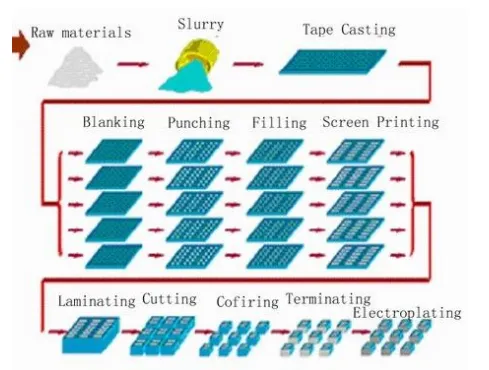
① Casting slicing: the dielectric layer of the Coulomb type electrostatic chuck is free of doping conductive materials, and the ceramic powder, solvent, dispersant, binder, plasticizer, sintering additives and other components can be mixed to prepare a stable slurry, and the ceramic green with a certain thickness can be coated, dried and sliced on the casting machine by a scraper. The JR type electrostatic chuck also needs to add a certain resistance regulating agent (conductive material) to the J-R layer resistance to the required range of function, and then the casting molding is prepared into green.
② Screen printing: screen printing is mainly used for the preparation of the electrode layer. In the printing process, the conductive paste is first poured on one end of the screen plate, and then under the action of the screen printer scraper, the conductive paste is deposited on the base through the mesh of the screen plate, when the printing scraper is scraped through the entire screen plate and ensure that the silver paste is filled with the screen hole, a printing process can be completed.
③ Laminated hot pressing: the raw tiles are stacked in accordance with the required order (base layer, electrode layer, dielectric layer) and the number of layers at a time, and then the multi-layer raw tiles are connected together under a specific temperature and pressure to form the required complete green. It should be noted that in the laminating process, the generated pressure should be evenly distributed on the entire green surface to ensure that the entire green shrink evenly after pressure.
④ Co-firing: Finally the complete green billet is placed in the sintering furnace for integrated sintering. In this process, it is necessary to formulate a suitable rising and cooling curve to ensure the flatness and shrinkage control in the sintering process. It is understood that in the sintering process of NGK in Japan, the shrinkage rate of powder sintering can be controlled at about 10%, while the shrinkage rate of most domestic manufacturers is still greater than or equal to 20%.
At present, the global semiconductor wafer electrostatic chuck market is highly monopolized by Japanese enterprises such as SHINKO (Shinko Electric), TOTO, NGK, Kyocera, etc. The development time of China's electrostatic chuck industry is relatively short, and it is still in the initial stage. At present, in addition to the need to further develop higher purity, higher performance raw material ceramic powder and more efficient and stable production processes, it is also necessary to consider the needs of various specific application scenarios to optimize the design of the structure to meet the increasing size of the bearer wafer specifications and the increasing demand for temperature uniformity control.
Fountyl Technologies PTE Ltd, is focusing on semiconductor manufacturing industry, main products include: Pin chuck, porous ceramic chuck, ceramic end effector, ceramic square beam, ceramic spindle, welcome to contact and negotiation!