


News

Etch etching equipment domestic and foreign market analysis
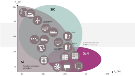
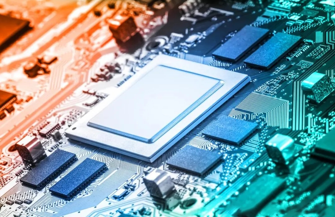
In 2018, the global market size of etching equipment is as high as about 10 billion US dollars, and with the reduction of chip process nodes, the steps of etching are further increased, and the demand for etching machines is increasing. China will become the world's largest semiconductor equipment market, while the etching, deposition, cleaning, testing equipment have achieved domestic breakthroughs. Compared with the quarterly decline of the global semiconductor market, China's semiconductor equipment market has shown a booming trend.
Etching equipment industry concentration is high, Pan forest semiconductor company occupies half of the etching machine market share. With the advancement of semiconductor technology, the number of device interconnect layers increases, and the use of media etching equipment continues to increase, Panglin Semiconductor takes advantage of its lower equipment cost and relatively simple design, and gradually exceeds TEL and other companies in the 65nm and 45nm equipment market, occupying more than half of the global market and becoming the industry leader. According to The data of The Information Network, Panglin Semiconductor Company's market share in the etching equipment industry has gradually increased since 2012, from about 45% in 2012 to about 58% in 2019, mainly replacing the market share of Tokyo Electronics Company. Tokyo Electron's market share fell from 30 percent in 2012 to 18 percent in 2019, but it remained in second place. Applied Materials is consistently in third place, accounting for about 19 percent of the market in 2017. The top three companies accounted for 94% of the total market share in 2017, with high industry concentration and obvious technical barriers.
(1) Introduction of Lam Research and its equipment
With the development of miniaturization of chips, more complex and slender feature patterns need to be created in the development of integrated circuits, so the dielectric (insulation) and metal (conductive) materials added during the deposition process need to be selectively removed. The main technique of reactive ion etching is to bombard the wafer surface with ions (charged particles) to remove material. For smaller key features, atomic layer etching is a common means, and ALE can remove several atomic layers of material. Lam Research produces a range of equipment for etching different materials.
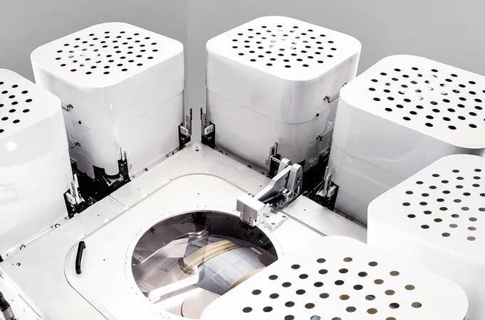
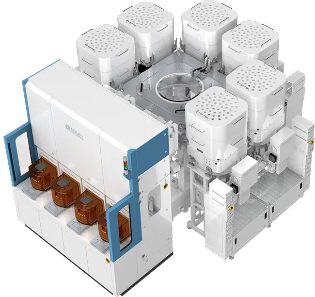
Lam Research is one of the oldest manufacturers of etching equipment, constantly updating corresponding etching equipment to keep up with the pace of semiconductor development. As shown, the company's initial business was the production of etching equipment, the first etching machine product, AutoEtch 480, was introduced in 1981, and the etching equipment supporting the 1.5μm process was developed in 1982, and the etching equipment supporting the 0.8μm process was developed in 1989. The company developed the first ICP dry etching equipment in 1992, the first dual-frequency ICP medium etching equipment in 1995, which can be applied to 350nm process chips, and the 2300 series products in 2000, which can be applied to 180nm chip processes. The figure shows Lam ResearchAutoEtch 690 product diagram and Lam Research 2300 product diagram respectively.
At the end of 2014, the company added ALE function to its Flex series of media etching system 350nm, which can be mainly applied to low k and ultra-low k mixed media and 3DNAND high aspect ratio aperture, groove and contact. The system uses the company's advanced Mixed Mode Pulse (AMMP) technology. The high selectivity of AMMP technology enhances ALE's etching effect, enabling ALE dielectric films, such as silica, to be used in next-generation logic chips and foundry operations. In addition, the company's Kiyo series of products also have ALE function, mainly for FinFET and three-gate, 3DNAND and high k dielectric/metal gate etching.
Dielectric etching mainly etches patterns on insulating materials to form a barrier between conductive parts of semiconductor devices. For advanced devices, these structures can be very tall and thin, involving complex, sensitive materials. Even at the atomic level, a slight deviation from the target feature profile can negatively affect the electrical performance of the device. To precisely create these challenging structures, Lam Research offers the Flex ® Product Family, a differentiated technology and application-focused capability for critical dielectric corrosion applications, as shown in the figure.
Uniformity, repeatability and tunability are achieved by a unique multi-frequency, small volume, restricted plasma design, and the Flex family of products guarantees continuous plasma generation, continuous etching of critical sizes, and increased productivity and yield.
Conductor etching is primarily used to form electrically active microstructures within semiconductors, where even small changes can create electrical defects that affect the performance of the device, and in the fabrication of integrated circuits, with the development of the nuance of key dimensions, so much so that the etching process is pushing the boundaries of the fundamental laws of physics and chemistry. Lam Research has designed the Kiyo R Product Family (Kiyo R Product Family) to accurately ensure the etching of key dimensions and key patterns, ensure the electrical performance of devices, and improve productivity, as shown in the figure.
Kiyo's patented Hydra technology in its products improves critical dimension (CD) consistency by correcting for input mode variability and enhances atomic layer etching capability through plasma. ALE) to achieve production-worthy atomic-scale variability control.
In dry etching, the process of using plasma etching to remove silicon or other materials deep in the silicon wafer is collectively referred to as deep silicon etching. These etches are mainly used in deep grooves for pixel isolation in CMOS image sensors, grooves in power devices and other devices, TSV and other critical devices with high aspect ratio characteristics. During processing, these key structures are mainly formed through continuous etching of multiple materials, but each new material will change during the etching process. For deep silicon etching technology, Lam Research has developed the Syndion R Product Family (Syndion R Product Family), which provides fast process switching and depth control, which can better achieve uniformity control on different silicon wafers, as shown in the figure. With its good process control characteristics, this series of products can not only be applied to traditional single step corrosion processes, but also has a good application prospect in the development of rapid alternating processes, which can ensure the minimum damage and provide accurate depth uniformity.
The metal etching process plays a key role in joining the individual components that form integrated circuits, such as forming wires and electrical connections. These holes can also be used to drill through metal hard masks whose mode features are too small for conventional masks, allowing for a continuous contraction of the characteristic dimension. In order to achieve these critical etching steps, Lam Research has introduced the Versys@Metal Product Family, a technology family that greatly increases the production capacity of products. Its unique symmetrical cavity structure can also independently control the uniformity of the device CD and profile, as shown in the figure.
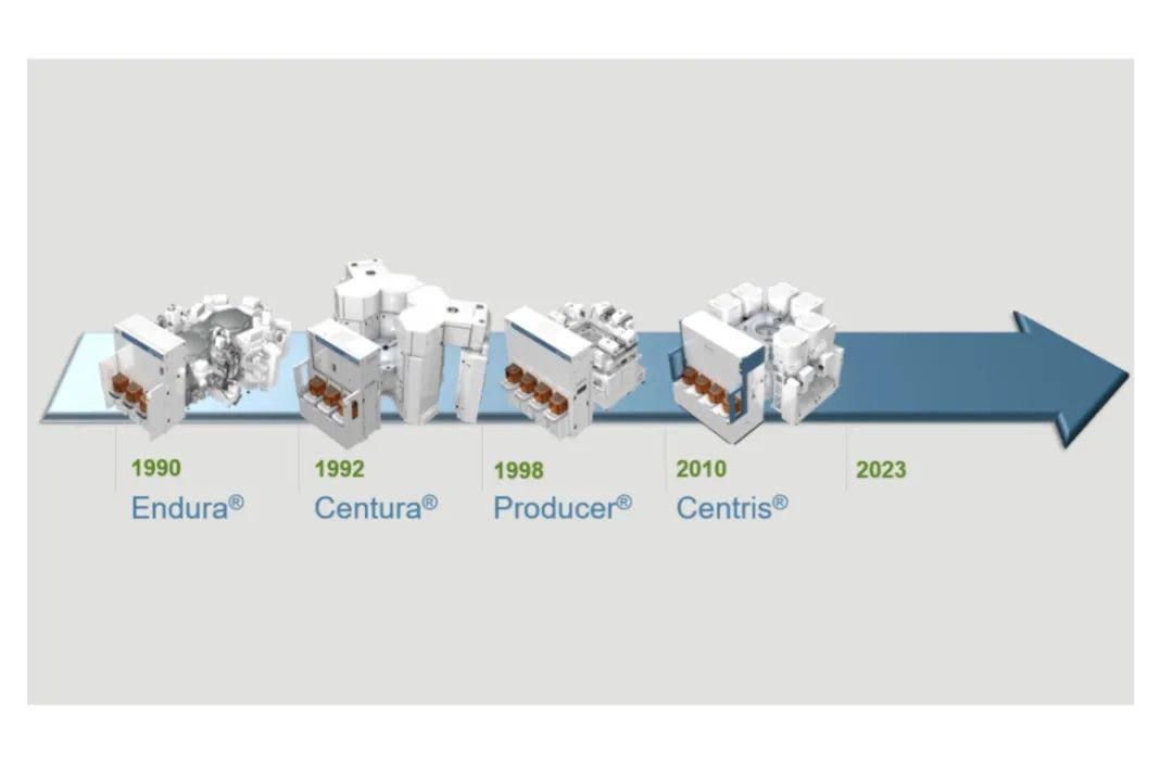
(2) Applied Materials Company and its equipment
As the world's largest semiconductor equipment and service provider, Applied Materials has a deep technical accumulation in etching equipment, the company's etching equipment has a long history of development, leading many technological advances in history. As early as 1997, the company launched a DPS etching device for integrated circuits, Silicon Etch DPSCentura, which can be applied to the chip manufacturing process of 0.25μm and below. It is the world's leading silicon etching system and one of the most successful etching products in the industry.
In 1999, the company introduced Silicon Etch DPS PlusCentura, which can be used for 0.1μm and below. In July 2000, the company introduced MetalEtch DPS 300 and Silicon Etch DPS 300, 12-inch etching systems that support all dielectric, silicon and metal etching applications. Applied Materials' semiconductor etching equipment covers all industries from silicon etching to dielectric etching.
In response to the technological development of the semiconductor industry, Applied Materials continues to achieve technological innovation in the field of etching. In 2011, Applied Materials released a new etching system AppliedCentura® SilviaTM. The etching rate is increased by 40%, reducing the etching cost per wafer. From a technical point of view, the new technology makes the through-hole of the wafer smoother and has a higher aspect ratio. On July 13, 2015, Applied Materials announced the AppliedCen-trisTM Sym3TM etching system, a next-generation etching device with a new reaction chamber that enables atomic-level precision processes. In June 2016, Applied Materials made a new breakthrough in etching technology by launching the Applied Producer ®SelectraTM system, the industry's first ALE etching device, which helps reduce the size of 3D logic chips and memory chips by introducing new material engineering capabilities. The figure shows some products of Applied Materials.
(3) Tokyo Electron Ltd. Company and equipment introduction
Tokyo Electron Ltd. Tokyo Electron is a leading semiconductor equipment supplier in Japan, mainly selling flat panel displays and semiconductor equipment. In the FPD manufacturing equipment, the share of etching machine equipment reached 83%. In 2018, the global market share of flat panel display etching equipment reached 71%. Tokyo Electronics has always focused on core technology research and development, and has a deep history of research and development of etching equipment.
In 2001, Tokyo Electron Corporation acquired Supercritical Systems, a U.S. company, and acquired the 100nm process technology. In 2002, the plasma medium etching system TeliusTM was introduced, creating a 70nm process technology. In 2005, the company ranked first in the global market sales of plasma etching systems, and released 65nm and 45nm process technology products. In 2006 TeliusTM was equipped with the latest etching chamber SIn 2010 Tokyo Electronics launched a new plasma etching system C C M ^ {TM ^ J I. Combined with TactrasTMRLSATMEtch, this technology is a revolutionary plasma technology that enables non-damaging, low energy and high electron density etching. In 2011, Tokyo Electronics introduced the upgraded TactrasTMVigusTM plasma etcher, which can be applied to 20nm process products. In 2012, Tokyo Electronics China Kunshan plant successfully produced parts for flat panel display plasma etchers. In 2013, Tokyo Electronics launched the ICP plasma etching system for Gen8 panels, a new technology that has strong advantages in the production of large panels. In 2014, Tokyo Electronics introduced a low loss and high selection ratio etching system for 3DNAND flash memory and FinFET. In 2016, for the production of small and medium-sized high-definition flat panel products, Tokyo Electronics launched a new etching system. In 2017, Tokyo Electronics mass-produced and sold the ICP etching system, and the new system can meet the market's needs for high-resolution 4K and 8K, as well as large-screen tablets.
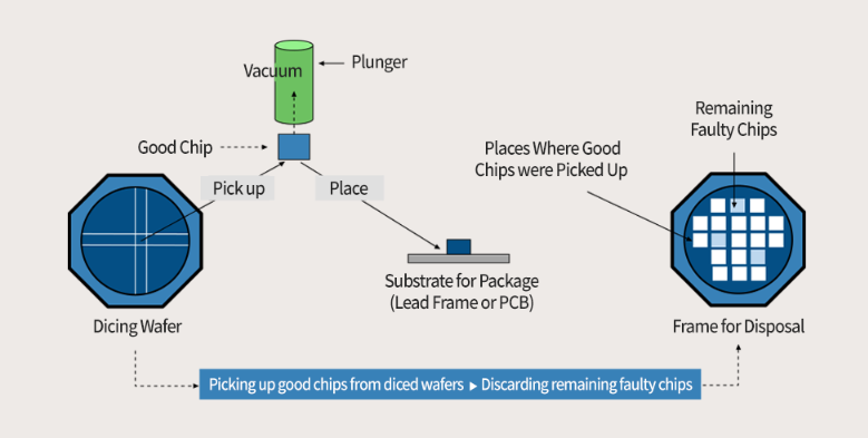
FOUNTYL TECHNOLOGIES PTE. LTD. was located in Singapore, we are focus on the research and development, manufacturing and technical services of precision ceramic parts in the semiconductor field for more than 10 years. our main product are ceramic chuck, ceramic end effector, ceramic plunger and ceramic square beam, and produces various of ceramics (porous ceramics, alumina, zirconia, silicon nitride, silicon carbide, aluminum nitride and microwave dielectric ceramics and other advanced ceramic) parts.