


News


Ten kinds of deposition technologies about PVD & PVD and CVD & AMAT PVD product Introduction
Film deposition is a very important technology in semiconductor manufacturing process, which is a series of processes involving the adsorption of atoms, the diffusion of adsorbed atoms on the surface and the coalescence of adsorbed atoms at appropriate locations to gradually form a film and grow. In the construction of a new wafer investment, 80% of the investment in the fab is used to purchase equipment. Among them, thin film deposition equipment is one of the core steps of wafer manufacturing, accounting for about 25% of the proportion.
Thin film deposition processes are mainly divided into physical vapor deposition and chemical vapor deposition. Physical Vapour Deposition (PVD) technology refers to the use of physical methods to vaporize a material source - a solid or liquid surface into gaseous atoms, molecules or partial ionization into ions under vacuum conditions, and through a low pressure gas (or plasma) process. A technique for depositing a thin film with a specific function on the surface of a substrate. The principle of physical vapor deposition can be roughly divided into evaporation coating, sputtering coating and ion plating, and specifically includes various coating technologies such as MBE. At present, physical vapor deposition technology can not only deposit metal film, alloy film, but also deposit compounds, ceramics, semiconductors, polymer films and so on.
With the development of technology, PVD technology is also constantly innovating, there are a lot of specialized technologies for certain uses, in this special inventory for everyone to introduce a variety of PVD technology.
Vacuum Evaporation coating technology
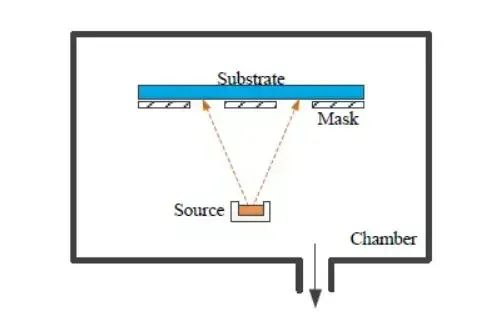
Vacuum evaporation coating is under vacuum conditions, the evaporation material is heated by the evaporator, so that it sublimates, the evaporation particle flow is directly directed to the substrate, and deposited on the substrate to form a solid film, or heating evaporation coating material vacuum coating method. The physical process is: using several energy methods to convert into heat energy, heating the plating material to evaporate or sublimate, and become gaseous particles (atoms, molecules or atomic groups) with a certain energy (0.1~0.3eV); When leaving the plating surface, gaseous particles with considerable velocity are transported to the substrate surface in a straight line flight with basically no collision. The gaseous particles that reach the surface of the matrix condense into nucleation and grow into solid phase films. The atoms that make up a film are rearranged or chemically bonded.
Electron beam evaporation technique
Electron Beam Evaporation is a type of physical vapor deposition. Different from the traditional evaporation method, electron beam evaporation can accurately use high-energy electrons to bombard the target material in the crucible, melting it and then depositing it on the substrate by the cooperation of electromagnetic field. Electron beam evaporation is commonly used to prepare Al, CO, Ni, Fe alloy or oxide film, SiO2, ZrO2 film, corrosion resistant and high temperature resistant oxide film.
Sputtering coating technology
Sputtering coating technology is to bombard the surface of the target with ions, and the phenomenon that the atoms of the target are hit is called sputtering. The atoms produced by sputtering are deposited on the substrate surface to form a film called sputtering coating. Gas ionization is usually produced by gas discharge, and its positive ions bombard the cathode target at high speed under the action of electric field, knock out the cathode target atoms or molecules, and fly to the surface of the substrate to be deposited into a film.
Rf sputtering technology
Rf sputtering is a kind of sputtering coating technology. The AC power supply instead of the DC power supply constitutes the AC sputtering system, because the frequency of the commonly used AC power supply is in the RF segment, such as 13.56MHz, so it is called RF sputtering.
Magnetron sputtering technology
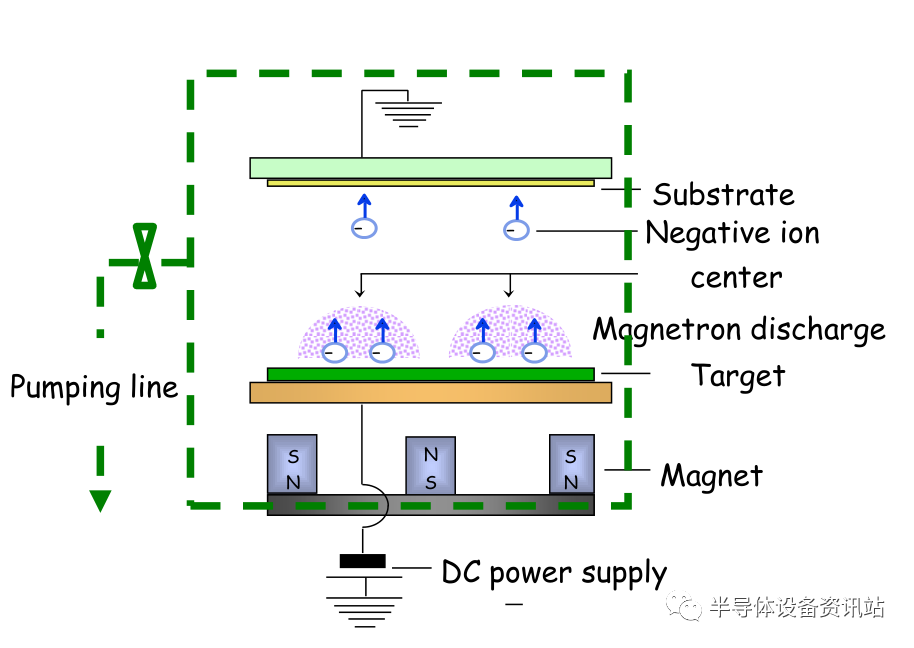
Magnetron sputtering technology belongs to PVD (physical vapor deposition) technology and is one of the important methods for preparing thin film materials. It is the use of charged particles accelerated in the electric field has a certain kinetic energy, the ion is directed to the sputtered material made of the target electrode (cathode), and the target atom sputtered out to make it move along a certain direction to the substrate and deposited on the substrate into a film method. The magnetron sputtering equipment makes the coating thickness and uniformity controllable, and the prepared film has good density, strong adhesion and high purity. This technology has become an important means to prepare various functional films.
Ion coating technology
Ion plating is a new coating technology developed on the basis of vacuum evaporation plating and sputtering coating. Various gas discharge methods are introduced into the field of vapor deposition. The whole vapor deposition process is carried out in plasma. It includes magnetron sputtering ion plating, reactive ion plating, hollow cathode discharge ion plating (hollow cathode evaporation method), multi-arc ion plating (cathode arc ion plating) and so on. Ion plating greatly improves the particle energy of the film layer, and can obtain a film layer with better performance, which expands the application field of "film". It is a rapidly developing and popular new technology.
Multiple arc ion Plating (MAIP)
Multi-arc ion plating is a method of direct evaporation of metal on the solid cathode target by arc discharge. The evaporation is the ion of the cathode substance released from the bright point of the cathode arc, and then deposited on the surface of the substrate as a film.
Molecular beam epitaxy (MBE)
Molecular beam epitaxy (MBE) is a newly developed epitaxy film making method, which is a new technology for growing high-quality crystal films on crystal substrates. Under ultra-high vacuum conditions, the vapor generated by the furnace heated with various required components, the molecular beam or atomic beam formed after the collimation of the small hole, is directly injected into the single crystal substrate at the appropriate temperature, and the molecular beam is controlled to scan the substrate, so that the molecules or atoms can be arranged layer by layer "long" on the substrate to form a film.
Pulsed laser Deposition (PLD)
Pulsed Laser Deposition (PLD), also known as pulsed laser ablation (PLA), is a type of laser bombardment of an object, and then the bombarded material is deposited on a different substrate. A means of obtaining a precipitate or film.
Laser molecular Beam epitaxy (L-MBE)
Laser molecular beam epitaxy (L-MBE) is a new film preparation technology developed in recent years, which is an organic combination of molecular beam epitaxy and pulsed laser deposition technology, and laser evaporation coating technology under the condition of molecular beam epitaxy.
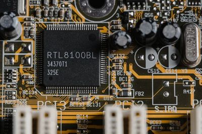
At present, the key PVD equipment in the chip manufacturing process mainly includes Hard Mask PVD equipment, copper interconnection (CuBS) PVD and aluminum liner (Al PAD) PVD, mainly using sputtering coating technology.
1, Comcept of PVD and CVD
PVD: Physical Vapor Deposition (PVD), also known as physical vapor deposition technology, is a thin film preparation technology that depositates materials on the surface of objects by physical methods under vacuum conditions. The coating technology is mainly divided into three kinds: vacuum sputtering coating, vacuum ion coating and vacuum evaporation coating. Can meet the coating needs including plastic, glass, metal, film, ceramic and other substrates.
CVD: Chemical Vapor Evaporation (CVD), also known as chemical meteorological deposition, is a method that refers to the gas reaction at high temperatures, the thermal decomposition of metal halides, organometrics, hydrocarbons, etc., hydrogen reduction or the biochemical reaction of its mixture of gases under high temperatures to precipitate inorganic materials such as metals, oxides, carbides, etc. It is widely used in heat-resistant material layer, high purity metal production and semiconductor film production.
2、Physical Vapor Deposition (PVD) process
1) Vacuum sputtering coating: When high-energy particles are accelerated by the electric field, they impact the solid surface, and the solid surface atoms/molecules exchange kinetic energy with these high-energy particles, thus flying out of the surface phenomenon called sputtering. According to the difference in the way of injection, it is divided into cathode and anode sputtering, three or four stage sputtering, high frequency sputtering, biased sputtering, asymmetric AC sputtering, adsorption sputtering, etc., and the most commonly used is magnetron sputtering.
2) Vacuum evaporation coating: It is a method of heating and evaporating the solid material in vacuum to condense it on the substrate surface to form a film.
3)The basic principle of vacuum ion plating is that under vacuum conditions, some plasma ionization technology is used to partially ionize the plating atoms into ions, while producing many high-energy neutral atoms, and negative bias is added to the plated substrate. In this way, under the action of deep negative bias, ions are deposited on the surface of the substrate to form a thin film.
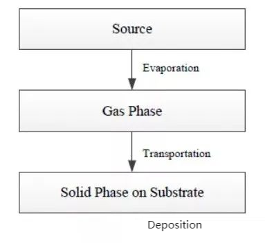
The PVD deposition process can be roughly divided into three parts: evaporation of the plating, migration of the plating and deposition of the plating
3、CVD (Chemical Vapor Evaporation) process
Chemical Vapor Evaporation (CVD) is chemical meteorological deposition, which refers to the gas phase reaction under high temperature. This process mainly refers to the gas phase reaction under high temperature, and is widely used in heat-resistant material layers, the production of high purity metals and the production of semiconductor films.
CVD reactive material sources can be divided into:
- Gaseous material sources: substances that are gaseous at room temperature (H2, N2, CH4, Ar, etc.). When the gaseous material source is used, the layer device system is greatly simplified because only the flow rate of the reaction gas needs to be controlled by the flow meter, rather than the temperature.
- Liquid material sources: reactive substances that are liquid at room temperature, such as TiCl4, CH3CN, SiCl4 and BCl3. The amount of liquid material source entering the deposition chamber is controlled by controlling the carrier gas and heating temperature when the liquid material flow is used.
- Solid material sources: Substances that are solid at room temperature, such as AlCl, NbCl5, TaCl5, ZrCl5 and HfCl4. Because this kind of material needs to sublimate the required amount of steam at a higher temperature, the heating temperature and the carrying capacity need to be strictly controlled when using this kind of process.
AMAT PVD product introduction
The PVD deposition process is used in semiconductor manufacturing to make ultra-thin, ultra-pure metal and transition metal nitride films for a variety of logic and memory devices. The most common PVD applications are aluminum plate and pad metallization, titanium and titanium nitride liners, barrier deposition, and copper barrier seed deposition for interconnect metallization.
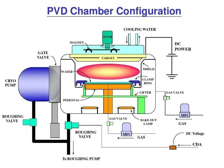
The PVD film deposition process requires a high-vacuum platform on which the PVD deposition process is integrated with degassing and surface pretreatment technologies to obtain the best interface and film quality. Applied Materials' Endura platform is the current industry gold standard for PVD metallization.
Fountyl Technologies PTE Ltd, is focusing on semiconductor manufacturing industry, main products include: pin chuck, ring groove chuck, porous ceramic chuck, ceramic end effector, ceramic beam&guide, ceramic structural part, welcome to contact and negotiation!