


News


The main method and technology of Die Bonding
What is the Die bonding
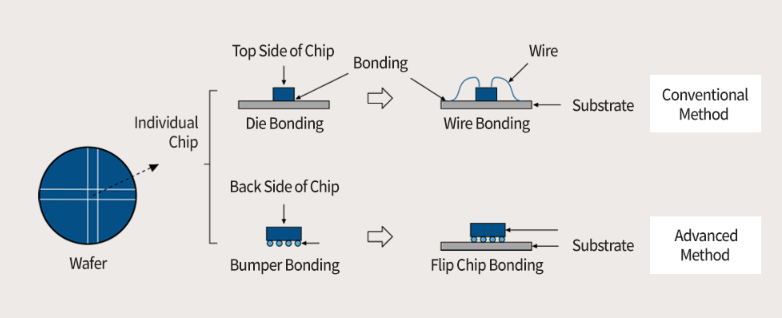
In the semiconductor process, "bonding" refers to the connection of a wafer chip to a substrate. Connection can be divided into two types, namely traditional method and advanced method. Traditional methods include chip connections (or chip connections) and wire connections, while advanced methods include flip chip connections developed by IBM in the late 1960s. Flip chip bonding is a method that combines die bonding and wire bonding, and connects the chip and substrate by forming a convex on the chip liner.
Just as an engine is mounted on a car to provide power, the chip wiring is connected to the outside world by attaching a semiconductor chip to a lead frame or printed circuit board (PCB). After the chip is connected, it should be able to withstand the physical pressure generated after the package, and can dissipate the heat generated when the chip is working. When necessary, it must maintain constant conductivity or achieve a high level of insulation. Therefore, as chips get smaller and smaller, bonding methods become more and more important.
The process of Die bonding
In the traditional chip bonding method, the first thing to do is to coat the packaging substrate with adhesive, and then put a chip on it, the chip has the pin side up. Under the flip-chip bonding process as an advanced package, the pin side of the chip is down, and a small bump of the solder ball on the pin is attached to the liner of the chip. In both methods, the assembled unit passes through a tunnel called temperature reflux, which can adjust the temperature over time to melt the adhesive or solder ball. It is then cooled to attach the chip (or bump) to the substrate.
Picking&Placing process for chip
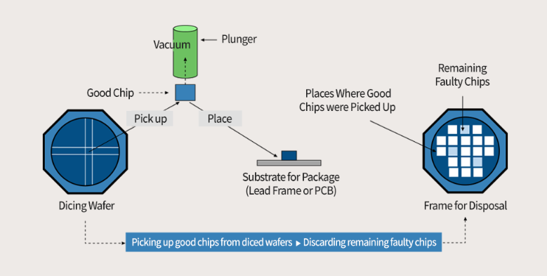
Removing the chip attached to the tape individually is called a "Pick." When the nozzle removes the chips from the wafer, they are placed on the surface of the package substrate called "Place". These two actions are known as the "pick and place "Piack&Place process. This process can also be used to sort good chips by entering the wafer test results (Go/No Go).
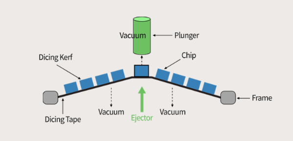
Chip suppress
Each chip that completes the slicing process and is attached to the tape by a weak adhesive. At this point, it is not so easy to pick up the chips that are placed horizontally on the dicing tape one by one. This is because even using a vacuum cleaner to pull it up is not easy to fall off, if forcibly pulled out, it will cause physical damage to the chip. Therefore, "Ejection" and" ejection "become an easy way to pick up the chip. A catapult is used to apply physical forces to the target chip, causing it to differ slightly in step size from other chips. Pop the chip out from the bottom and pull the chip up from above with a vacuum band plunger. At the same time, vacuum the bottom of the tape to make the sheet flat.
Die bonding process
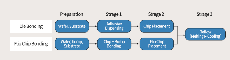
When epoxy resin is used for mold bonding, a very small amount of epoxy resin is precisely applied to the substrate by dispensing. After the chip is placed on it, the epoxy resin hardens at 150 to 250°C by reflux or curing in order to bond the chip and the substrate together. If the thickness of the epoxy resin applied is not constant, warping that causes bending or deformation may occur due to differences in the coefficient of thermal expansion. For this reason, control of the amount of glue is very important. But as long as epoxy resins are used, any kind of warping will occur. This is why more advanced bonding methods using die film (DAF) have recently been preferred. Although DAF has some expensive and difficult to handle disadvantages, its thickness can be well controlled, and it simplifies the process, so its use is gradually increasing.
Die attach film (DAF) bonding
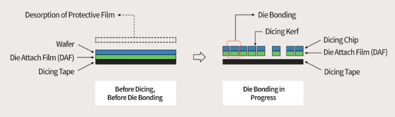
DAF (Die Attach Film) is a thin film attached to the bottom of the mold. With DAF, the thickness can be adjusted to be thinner and constant than when using polymer materials. It is widely used not only in chip-to-substrate bonding, but also in chip-to-chip bonding to create multi-chip packages (MCP). From the structure of the chip, the DAF at the bottom of the chip is to hold the chip, and the slicing tape is to pull the DAF below it, and the adhesion is weak. In order to perform mold bonding in this structure, the mold should be placed on the substrate after the chip and DAF are removed from the dicing strip at one time, without the use of epoxy resin. This process skips the dispensing procedure, which is not only faster, but also perfectly avoids problems caused by uneven glue thickness. When using DAF, some air can penetrate the film, causing problems such as film deformation. In particular, equipment that handles DAF requires high precision. However, using daf is the preferred method because it reduces the absence rate and increases productivity because it simplifies the process and increases thickness uniformity.
Fountyl Technologies microporous vacuum chuck can be used with Japanese, German, Israeli, American and domestic equipment, with very superior product performance and good one-to-one service.